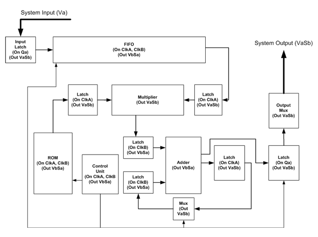
| The timing diagram in Figure 1 illustrates how the two-phase clock ("A" and "B")
is distributed to the primary filter components. The "On" designation
indicates which clock the module receives, and the "Out" designation indicates
the timing "strength" of
the output signal. |

Figure 1: System Timing Diagram
For further details on the complete system design, please refer to the Block
Diagram section.