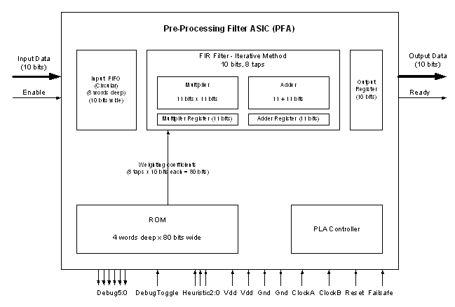
Overview : Project Proposal In this project, we will implement an FIR pre-processing filter ASIC for use in a digital hearing aid application. The overall system architecture is shown in Figure 1.
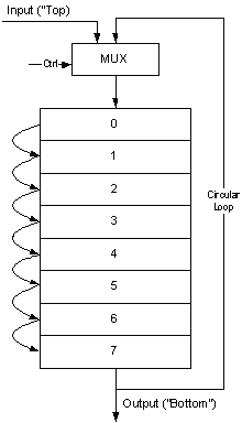
The system receives a 10-bit audio sample triggered by an enable flag, processes the sample, and outputs a 10-bit filtered value along with a ready flag to next stage of the hearing aid system. All samples are stored as two’s complement fixed point data. The exact placement of the decimal point remains to be determined. The FIR filter has 8 taps, processes 10-bit wide data, and implements the following equation: Due to space limitations, only a single multiply-and-accumulate unit is provided. Instead, the PLA controller will iterate the filter once for each tap. Both the adder and the multiplier operate on 11-bit data instead of 10 bits. This extra bit added at the most significant end gives us the ability to slightly overflow on one stage of the filter, in the hopes that a later filter coefficient will reduce the result back into the normal 10-bit range. At the end of the filter, however, all results will be truncated to fit into the original 10-bit format. When only 10-bits are available for input into the filter (such as during the first iteration), the most significant bit will be sign-extended from the less-significant 10. The weighting coefficients are loaded from an on-chip ROM which can store 4 distinct sets, where each set contains 8 10-bit coefficients. The external “heuristic” pins are used to select the desired coefficient set. For simplicity, this ROM is organized as 80 bits wide, so the entire set of coefficients can be retrieved in a single cycle. It is likely that 1 of the debug pins will be used as an input to toggle the remaining 6 outputs between two different resources, such as the current PLA state and the current value of the FIFO output. The Failsafe pin is used to disable the entire filter, so that the input signal is merely copied to the output pins. The Reset pin is used to reset the PLA and clear system buffers (such as the FIFO and other registers) so that the system output is not contaminated by leftover values from previous filter iterations. The input FIFO is used to buffer as many input data samples as there are taps in the filter. This circular FIFO is cycled once as the FIR filter iterates through its computation. Then, at the end of the filter computation, the oldest value in the FIFO is replaced by a new input sample, and the filter cycle begins again. The design of the input FIFO is shown in Figure 2.
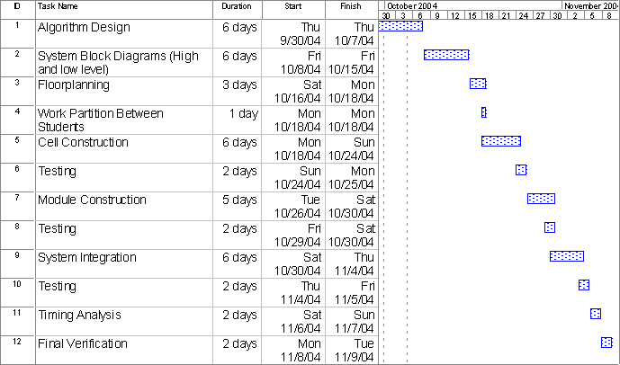
The project timeline for implementation is shown in Figure 3.
|


