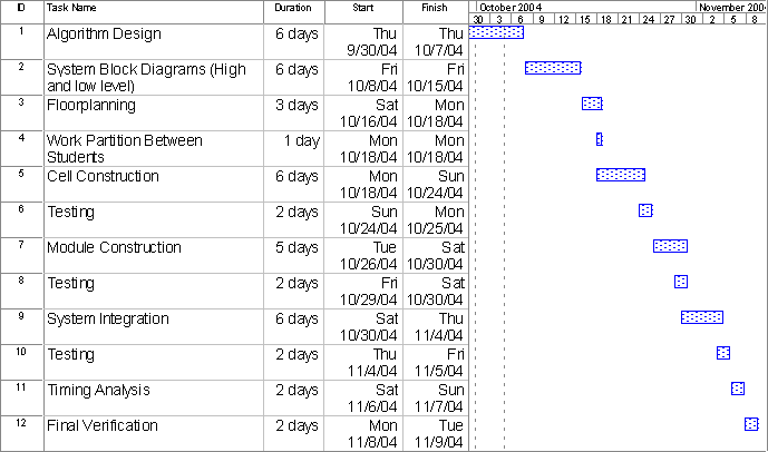
Overview : Progress Report 2 – November 2nd, 2004 In this project, we are implementing an FIR pre-processing filter ASIC for use in a digital hearing aid application. The original project timeline from the proposal is shown in Figure 1.
When compared to the original timeline, the project is on or slightly ahead of schedule. As of November 2nd, most key tasks have been completed. Recently, high-level modules have been constructed and tested, including the adder, multiplier, ROM, system controller, and various latches and multiplexers. Full system integration using these modules has been performed and verified in the simulator. While not yet in the final pad frame, the modules are in their final relative locations, and I/O lines have been routed to the appropriate edge of the design. To complete the project, several items must still be completed. Specifically, the “failsafe” data
bypasses need to be added and the FIFO and ROM modules need to be enlarged. This will increase
the number of filter taps for higher quality and also maximize chip utilization. Once complete,
more rigorous testing will be performed, including final checks of the chip density and substrate
contacts. Finally, the design will be inserted into the pad frame and verified again. These tasks
should be completed on-schedule, and thus the original project timeline will be valid for the
remainder of the project. |
