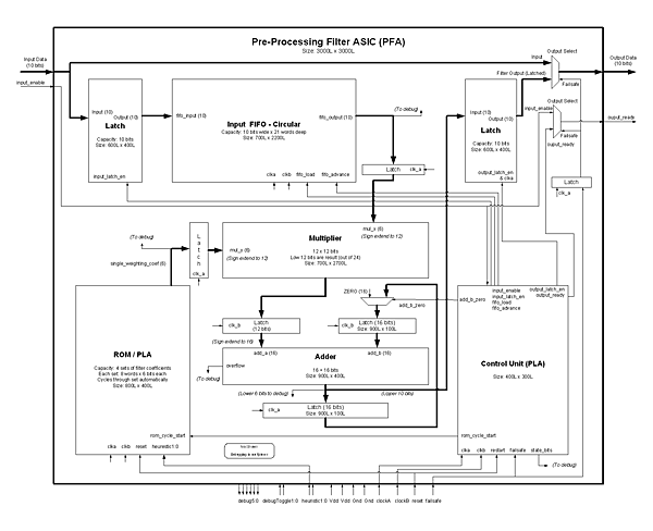
In the final system, 10 bits worth of two's-complement input data is delivered to the
input ports. The control unit is notified of the delivery of new data by asserting the
input_enable pin. Under the control of the control unit, the new data is first latched
and then loaded into the top element of the circular FIFO. The FIFO stores 21 10-bit
wide data elements,
and
has the capability to load new data either from the FIFO output (making it circular),
or from the system input pins.
At the same time the new data element is loaded into the FIFO, the ROM decodes the 2-bit
heuristic input line to determine which filter coefficients are to be
applied to the incoming data.
After the new data is loaded, the control unit sends a signal to both the ROM and FIFO
to start outputting filter coefficients and data elements at a rate of 1 element per
cycle. The FIFO is configured in a circular mode, so no data is lost. Each of these outputs
are first latched, and then delivered to a 12-bit multiplier.
The multiplier computes the product of both the filter coefficient and truncates the output
to the least-significant 12 bits. This output is then latched, sign extended, and delivered
to a 16-bit adder. The 16-bit adder was designed to have sufficient "headroom" to reduce
the
possibility
of arithmetic overflow. The second input to this adder is selected by the control unit.
Because the goal of this filter is to perform a multiply and accumulate, the second adder
input is either a set of zeros for the initialization state, or the latched output of
the previous addition operation. Regardless of which option is selected, the adder output
is latched
There are two options for the system output. If the failsafe input pin is enabled, the
entire filter is disabled such that the input data and trigger signal are merely
copied to the output pins. If failsafe is not enabled, the output of the adder
is delivered to a dedicated output latched and saved for prolonged delivery to the output
pins. In addition, the output_ready pin is asserted by the control unit for 5 cycles.
The Reset pin is used to reset the PLA and clear system buffers
(such as the FIFO and other registers) so that the system initializes from a clean
state.
The Debug and DebugToggle I/O lines are described in the testing
section of this report.
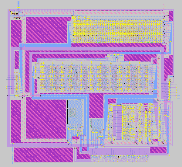
Figure 2 shows the final design as realized in MAGIC. |

