 |
Testing : IRSIM Functional Analysis
Normal Operation:
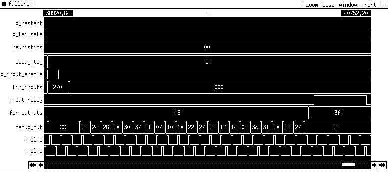
The most significant test result is an end-to-end test of the final design inside
the pad frame. This is shown in Figure 1. |

Figure 1: End-to-End Simulation [See also: The IRSIM .cmd
file that generated this output]
It is important to note that Figure 1 only shows a fraction of the full simulation
time. The first 20 simulation iterations are used simply to load the FIFO with data
samples. (Recall that this FIR filter is 21 taps long, and must iterate over all
the taps
in order to produce a single output coefficient). Thus, useful filter results are
first produced in the 21st iteration.
In this simulation, the input-enable pin is
asserted on the left side of the figure, indicating
that
a new
data sample
is
available
to
be
filtered.
The
FIR
filter
processes
the
data
over 21 clock cycles, and releases the filtered coefficient on the fir_output
lines. It signals that this data is available by asserting the output-ready line
for 5
cycles, as shown at the right side of the figure. The debug system is also active
in mode 2, which copies the FIFO output to the debug port. This debugging methodology
is described in more detail below.
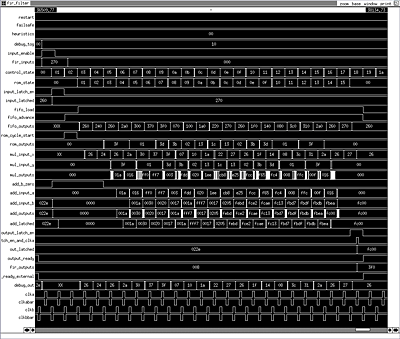
An alternate version of this same simulation is shown in Figure 2. This is an internal
simulation within the pad frame, and thus illustrates more of the internal signals.
|
Click on the figure for a full-sized view

Figure 2: Internal Simulation [See also: The IRSIM
.cmd file that generated this output]
This simulation clearly shows the progression of input data 0x270 from the input lines
through the FIFO, multiplier, and adder. At the end, the output-ready signal is asserted
and the output of 0x3F0 latched for safekeeping.
Failsafe Mode:
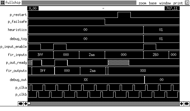
Figure 3 shows the failsafe mode in operation. When the failsafe signal is asserted,
the input-enable line and input data lines are copied directly to the output-ready
and output data lines.
|

Figure 3: Failsafe Mode
Debug Mode:
The filter design also includes a significant debugging component. Two debugging
mode input pins allow the operator to select between four different six-bit debugging
outputs. These modes are:
- The least significant 6 bits of the output latch. The most significant
10 bits (from the 16-bit output accumulator) is delivered normally to the
standard output pins. These bits provide additional precision for the resulting
filtered data.
- The six bits from the ROM, to view the filter coefficients being
delivered to the multiplier.
- The most significant six bits from the FIFO, to view the data being delivered
to the multiplier.
- An overflow signal from the adder, plus all 5 state bits from the control
unit.
The overflow signal is asserted if the most significant bit of the A adder input
is 1, the most significant bit of the B adder input is 1, and the most significant
bit of the sum is 0. Or, the overflow signal is also asserted if the most significant
bit of the A adder input is 0, the most significant bit of the B adder input
is 0, and the most significant bit of the sum is 1.
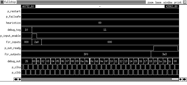
An example of the debug output mode is shown in Figure 4. Here, the debug system
is operating in mode 3, where the overflow indicator (not active) and the control
unit state bits are echoed to the output lines.
|

Figure 4: Debug Mode - Overflow and State Bits
|  |
|
