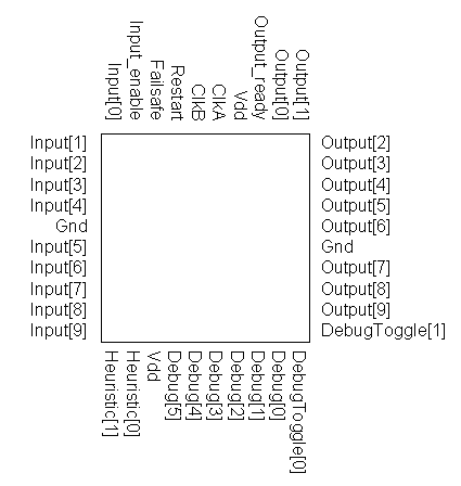
The pin assignments for the final chip are shown in Figure 1.

Figure 1: Chip Pin Assignments
Input Pins:
- Input[9-0]
- Input_enable - Signal that input data is available
- Failsafe - Enable failsafe mode and route input data directly to the output
- Heuristic[1-0] - Switch between ROM filter coefficients
Output Pins:
- Output[9-0]
- Output_ready - Signal that output data is available
Debugging Pins:
- DebugToggle[1-0] (Input) - Switch between 4 different debug modes
- Debug[5-0] (Output)
Standard Pins:
- ClkA
- ClkB
- Vdd (2)
- Gnd (2)
- Restart